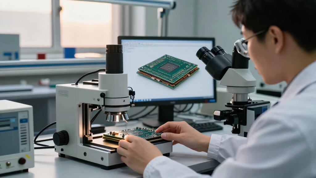
🔍 Read the full analysis: AI Chip Packaging, Explained: Where Dies And HBM Stacks Meet on ThorstenMeyerAI.com

Prime made for students and young adults
- Fast, free delivery for dorm and study essentials
- Prime Video and Amazon Music included
- Member-only deals
TL;DR
Modern AI accelerators combine multiple compute dies, stacks of high-bandwidth memory and a silicon interposer inside one package. Nvidia and AMD designs illustrate how packaging connects those components, while manufacturer statements indicate that advanced packaging and memory supply remain relevant constraints. The source does not establish how much those constraints affect prices or availability.
A November 22, 2026, hardware explainer from ThorstenMeyerAI.com describes how AI accelerators combine compute dies and stacked high-bandwidth memory (HBM) in a single package, using silicon interposers to connect them. The account matters because the speed of large AI systems depends not only on processor performance but also on moving data into compute units and manufacturing enough advanced packages and memory.
The article describes an accelerator package as a set of components rather than one piece of silicon. A package substrate connects the package to its module or circuit board. Above it, a silicon interposer provides dense wiring between compute dies and HBM stacks. The memory stacks sit beside the compute dies, and vertical connections called through-silicon vias (TSVs) link the DRAM layers within each stack.
Product details cited in the source show different approaches. Nvidia says its current Rubin GPU has two reticle-limited compute dies and 336 billion transistors. AMD says the MI350 Series integrates eight vertically stacked accelerator complex dies and two I/O dies; the source gives the MI355X a total of 185 billion transistors and eight 12-high HBM stacks. These are manufacturer specifications reported by the explainer, not independent measurements.
The article also traces the package into a rack. It cites Nvidia documentation describing NVL72 systems with 72 GPUs and 36 CPUs, alongside switch trays, power shelves and liquid cooling. Nvidia lists 120 kilowatts of cooling capacity for the GB200 NVL72. That system-level view shows why packaging is one part of a larger design involving memory, interconnects, power and cooling.
Why HBM Packaging Shapes AI Systems
Compute dies can perform operations only when data reaches them. HBM places memory close to the processor, while the interposer supplies many short connections between the memory and compute components. The source cites Nvidia product-page bandwidth figures rising from 900 GB/s for V100 to 19.2 TB/s for Rubin. Those figures compare specified products; they do not by themselves explain real-world performance, which also depends on the workload and system configuration.
Packaging also creates a manufacturing challenge. The source reports that TSMC’s CoWoS-S process supports silicon interposers up to about 2,700 square millimetres, described as 3.3 times reticle size. Larger packages can use CoWoS-L, which connects silicon bridges within a carrier. The source says TSMC’s chief executive described five-reticle-size production as real-world production on October 15, 2026, with larger sizes under development.
Memory capacity and packaging throughput can affect how quickly suppliers can build complete accelerators. SK hynix expects demand to exceed supply through 2030, according to the statement cited in the explainer. That is a company forecast, not a guarantee of shortages for every customer or product. The source provides no independent market data quantifying the effect on prices, delivery times or total system availability.
Popular right now

Apple AirPods Pro 3 Wireless Earbuds

Samsung 65-Inch Q8F QLED 4K UHD Smart TV (2025)

Dyson V15 Detect Cordless Stick Vacuum
As an affiliate, we earn on qualifying purchases.
From Silicon Layers to Rack Scale
The packaging process starts with a substrate that carries power and signals to the rest of the system. A silicon interposer sits above it, linking compute dies to HBM using a much denser network of connections than a conventional circuit board can provide. The compute dies perform the main calculations; the HBM stacks supply data close to those dies.
HBM is made by stacking DRAM layers on a base die and connecting them with TSVs. JEDEC’s HBM4 standard, published in April 2025 according to the source, allows stacks of four, eight, 12 or 16 layers and up to 64 GB per stack. SK hynix and Samsung statements cited in the article describe work on thinner layers and smaller gaps between chips. Those are manufacturer-reported product details, not an independent comparison of all available memory.
At rack scale, the components require connections between GPUs as well as cooling and power infrastructure. The source says Nvidia’s GB200 and GB300 NVL72 designs use 18 compute trays and nine NVLink switch trays, with liquid coolant running through cold plates attached to processors. Its discussion of AMD OAM modules and baseboards likewise shows how package-level design fits into a larger platform.
Limits of the Available Specifications
The source says Nvidia and AMD do not publish the physical dimensions of the dies, packages or individual memory stacks discussed, so its 3D models use schematic sizes. The layouts illustrate layer order and component counts; they should not be read as dimensionally accurate representations.
It is also unclear from the source how much advanced packaging capacity is available to each accelerator supplier, how shortages are allocated among customers, or how the cited supply outlook will affect prices and delivery schedules. Vendor specifications and forecasts are attributable statements, not independent confirmation of future system performance or availability.
The article’s product examples span different generations and platforms. Its bandwidth figures and transistor counts are product-specific figures, not direct measures of comparable performance. The source does not provide a common benchmark, nor does it quantify how much of any system bottleneck comes from memory, packaging, compute, networking or power.
Tracking Packaging and Memory Supply
The next useful indicators are updated product specifications, announcements about packaging capacity, and memory suppliers’ reports on production and demand. TSMC’s stated work on larger CoWoS-L packages and the development of taller HBM stacks point to ongoing changes in how much memory and compute can fit into a package.
For buyers, the practical test will be whether manufacturers can deliver complete systems at the scale and schedule customers need. Future availability and price effects remain uncertain; the source does not give a timetable for those outcomes or independent estimates of supply.
Key Questions
What does HBM mean in an AI accelerator?
HBM means high-bandwidth memory. It is DRAM arranged in vertical stacks and connected through the silicon with TSVs, placing memory close to the accelerator’s compute dies.
What does the silicon interposer do?
The interposer provides dense wiring between compute dies and HBM stacks. It connects the components within the package rather than performing the main computations itself.
Why can packaging limit AI accelerator supply?
Advanced packages need specialized interposers and assembly processes, as well as suitable HBM. The source describes packaging capacity as a production bottleneck, but does not quantify its effect on delivery times or prices.
How many GPUs are in an Nvidia NVL72 rack?
The source cites Nvidia documentation describing 72 GPUs and 36 CPUs in the NVL72 configuration, alongside switch trays and cooling equipment.
Are the source’s 3D package models to scale?
No. ThorstenMeyerAI.com says the models show layer order and component counts but use schematic dimensions because Nvidia and AMD do not publish the physical measurements cited.
Source: ThorstenMeyerAI.com